IJCRR - 13(8), April, 2021
Pages: 54-57
Date of Publication: 25-Apr-2021
Print Article
Download XML Download PDF
Efficient Neural Recording Amplifier for Brain Machine Interface
Author: Gunda Akanksha, Kaipa Sahithi, Lavanya Maddisetti
Category: Healthcare
Abstract:Introduction: In recent years, neural system study has become a fruitful approach in diagnosing neurological diseases. Brain signals being at very low potentials pose a difficulty to study them. Fault analysis of those signals may lead to improper diagnosis of the diseases. So, amplification of the brain signal is required. The amplified signal is prone to noise. Objective: To meet the limitations of the neural acquisition system a novel design for ultra-low noise neural recording amplifier is discussed in this paper. Methods: Characterization of transistors is the technique used to design the amplifier. The amplifier is designed in a standard 0.18µm Complementary metal oxide semiconductor process (CMOS). Results: The amplifier achieved a gain of 43.6dB with a total power consumption of 26.29µW and input-referred noise of 313.6pVrms.
Keywords: Brain-machine interface, Neural amplifier, Operational transconductance amplifier, Band pass filter, Input referred noise, Gain
Full Text:
Introduction
Ease of recognition of neural syndrome is made possible by following the procedural and standard methods such as cortical stimulation or transcranial stimulation. Similar to pacemakers the cortical simulation is nothing but the insertion of electrodes into the cortical areas of the brain which is in contrast to the deep brain stimulation which inserts the electrodes into deeper parts of the brain. But the transcranial stimulation just collects the neural information through the electrodes implanted of the scalp.1,2 All these approaches can be used to assist with the recovery of patients who suffered from motor neuron syndromes and neurological defaults. And these approaches also help paralyzed patient move a computer cursor by thoughts alone.3,4 But these approaches are limited to large equipment so a modern approach is made into practice which overcomes the limitation of cortical stimulation. The modern technique is nothing but the implantation of chip/IC into the cortical areas of the brain.5 The chip/IC implanted is nothing but the neural recoding IC. The critical part of the neural recording IC is the neural recording amplifier (NRA) which is solely responsible for the ease of analysis of neural signals.6 The main aim of the neural recording amplifier is to strengthen the neural signal which is at a low potential to ease the analysis.
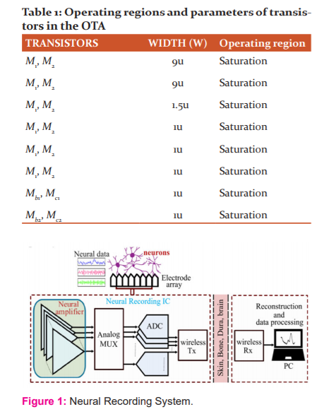
The setup of the implantable neural acquisition system is shown in figure1.7 The system consists of an internal unit and an external unit. The internal unit consists of a front-end processing stage that amplifies and digitizes neural signals from recording electrodes. The digitized neural data from the front-end processing stage is then processed by a digital signal processing module on the internal unit before the processed neural data is transmitted to the external unit via a wireless data telemetry system. The external unit receives the neural data and relays it to a remote device such as a computer. Due to the stringent requirement of less noise in the signal the goal of the paper is to decrease the noise. Chopper stabilization is a technique used to reduce the flicker noise components in the amplifier at low frequencies but it requires additional circuitry.8,9 Additional circuitry increases the area and also increases power consumption. The chopper technique also reduces the input impedance which leads to attenuation of the input neural signal.10 P-type metal oxide semiconductors are responsible for reducing flicker noise.11 So, the differential pair used in the design is a p-type metal oxide semiconductor. As the neural acquisition system is to be operated at low potentials, due to decrease in supply voltage power consumption will be increased.12 So noise power trade of is maintained in the circuits designed nowadays. The presented work outperformed the previous work in terms of noise-power trade-off.
Material and Methods
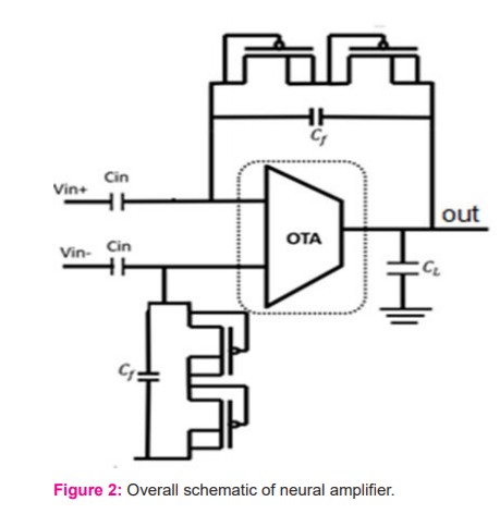
Amplification plays a major role in the analysis of the neural signal because the original signal occurs at a very low potential and small frequency. So, the proper choice of amplifier is to be done to achieve the design requirements. Amongst the variety of amplifiers available Operational Trans-conductance Amplifier (OTA) best suited for the neural signal analysis because the circuit can be stabilized or controlled by the input bias current. By this, it best fits the applications it is designed for. An Operational Transconductance Amplifier is a differential amplifier whose output current is controlled by input voltage sources. Thus, it is also called a voltage-controlled current source. Thus, the OTA amplifies the neural signal which is suitable for diagnosis. Even though the required amplification is achieved there may be some loss of information or adding additional information which may lead to errors in the diagnosis. So, not only the selection of amplifiers, the configuration of the amplifier must be done efficiently. So, a Bandpass filter (BPF) is integrated along with the designed OTA so that the loss or gain of erroneous information will not affect the original signal. The Bandpass filter is also used to adjust the neural signal between respective frequencies, which may be very helpful during the reverse treatment. The schematic of the overall neural amplifier is shown in figure 2. The design procedure of the OTA and the Band Pass Filter is altered to achieve more effective results. The design procedure is explained in the preceding section.
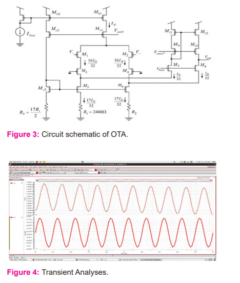
The circuit schematic of the OTA is shown in figure 3.13 The OTA consists of 18 transistors and each transistor has its importance which contributes to the overall gain of the amplifier. Overall transistor sizing and circuit modelling are based on the transconductance and bias current of the circuit. The gain and transconductance are related as
gm =2π.fUG.CL
Where fUG is the unity-gain bandwidth and CL is the load capacitance.
fUG (unity-gain bandwidth): The closed-loop gain and unity-gain bandwidth is related as
fUG=k.ACL.fL
where ACL is the closed-loop gain and its value is 20dB and the value of k is chosen to be 2. fLis the frequency of the input signal and the input signal range of bandwidth is 5.32kHz.
CL (load capacitance): The load capacitance is placed to insert a pole in the frequency response, which is due to the resistor-capacitor combination at the output of the amplifier. The resistor mentioned here is a virtual resistance shown by the amplifier at the output. Here we assumed a large value of capacitance i.e., 1nF. Considering all these the transconductance of the amplifier is obtained to be 251uS.
Characterization of the transistors
Characterizing is done to know the unknown parameter by considering a key parameter as a reference, here transconductance is considered as the reference. In our design length is fixed to 1µm. The combination of M1 and M2 is said to be a differential pair. These are constructed using P-type Metal Oxide Semiconductor transistors. PMOS is responsible to eliminate flicker noise (1/f noise). The width of the transistor is obtained to be 9um.M3 and M4 merely act as resistors so the width is the same as that of differential pair.M5 and M6 act as tail transistors so current is divided equally among them and thereby the widths of these transistors are same, and these are again characterized using above procedure. The current flowing from Ibias to the current source is the same as that of Mb2 and Mc2. Current flowing in Mb1 and Mc1 is twice as that of current in differential pair. The transistors M7,M8,M9,M10,M11,M12 form the second stage and thus the gm for this is again 251uS and the respective widths are obtained. The widths and lengths of all the transistors obtained by characterization are shown in Table 1.
From table 1, it is clear that all the transistors are in the saturation region. On setting the width of transistors as in the above table, the gain obtained is 53.2dB. The power consumption is 26.295uW. As discussed earlier to reduce the noise a BPF is integrated into the designed OTA to limit the noise. The BPF not only limits the noise but is also used to maintain the neural signal bandwidth.
RESULT AND DISCUSSION
The BPF is integrated as the closed-loop configuration to the OTA. After integrating the BPF noise is reduced to the greater extents. The transistors used in the feedback path act as high pass filters and the transistors used at the input side act as low pass filters. The noise after using a BPF is 313.9pVrms. The power remains the same because band-pass filter transistors operate in the sub-threshold region and do not consume much power.
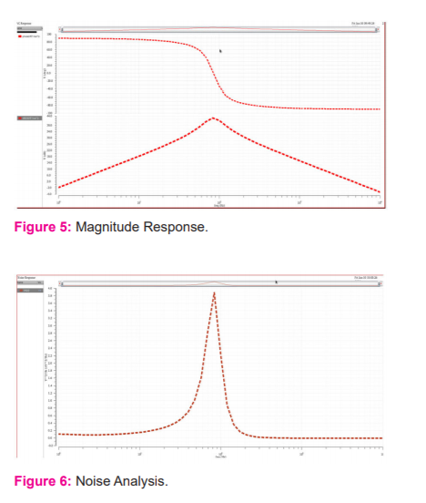
In the above graph, the first signal is the output voltage and the second signal is the power signal. For the voltage graph, the X-axis is time(ms) and the Y axis is voltage (v). For the power graph, the X-axis is time(ms) and the Y axis is watts(mW). figure 4 displays the transient response of the designed OTA with BPF which shows the potential of the output signal and the power consumption. The gain of the amplifier with BPF was observed to be 43.9dB.
In figure 5, the first graph is the phase graph and the below shows the gain graph. The X and Y-axes for the phase graph is time (ms) and degrees respectively. The X and Y-axes for the gain graph is time (ms) and gain in dB respectively. The input-referred noise of the OTA with BPF is 313.6pVrms. The noise analysis is shown in figure 6. Here, the X-axis is the frequency in hertz and the Y-axis is the noise factor.
Conclusion
Thus, the limitation to cortical stimulation is solved by using neural recording IC, and an effective way to design a low noise neural amplifier (the major part of neural recording IC) is discussed. The circuit parameters are modelled accordingly and a noise power trade-off is also maintained. The optimized design is applied to achieve the required gain by modelling transconductance. The high noise immunity is obtained by using a BPF and also the signal obtained is in the range of Local Field Potential frequencies. The overall gain of the neural recording amplifier obtained is 43.9 dB with a power consumption of 26. 29µW and the input-referred noise obtained is 313.6pVrms.
Acknowledgements: This research project was carried out at the Center for Advanced Computing Research Laboratory (C-ACRL), Vardhaman College of Engineering. The authors would like to thank the management and faculty for their constant support throughout.
Source of funding: NIL
Conflict of interest: NIL
Individual author’s contribution:
Author1 carried out the electrical parameters performance studies such as gain, designed the OTA and drafted the manuscript.
Author2 carried out the bandpass filter design, participated in the high noise immunity studies and helped to draft the manuscript. All authors read and approved the final manuscript.
References:
1. Mavoori J, Jackson A, Diorio C, Fetz E. An autonomous implantable computer for neural recording and stimulation in unrestrained primates. J Neurosci Methods 2005;148(1):71-7.
2. Guillory KS, Normann RA. A 100-channel system for real-time detection and storage of extracellular spike waveforms. J Neurosci Methods 1999;91(1-2):21-9.
3. Wessberg J, Stambaugh CR, Kralik JD, Beck PD, Laubach M, Chapin JK, et al. Real-time prediction of hand trajectory by ensembles of cortical neurons in primates. Nature 2000;408(6810):361-365.
4. Chapin JK, Moxon KA, Markowitz RS, Nicolelis MA. Real-time control of a robot arm using simultaneously recorded neurons in the motor cortex. Nat Neurosci 1999;2(7):664-70.
5. Sarpeshkar R, Wattanapanitch W, Arfin SK, Rapoport BI, Mandal S, Baker MW, et al. Low-power circuits for brain-machine interfaces. IEEE Transact Biomed Circ Syst 2008;2(3):173-83.
6. Majidzadeh V, Schmid A, Leblebici Y. Energy-efficient low-noise neural recording amplifier with enhanced noise efficiency factor. IEEE Transact Biomed Circ Syst 2011;5(3):262-71.
7. Punekar G, Gonuguntla V, Yellappa P, Choi JR, Vaddi R. A Low-power Low-noise Open-loop Configured Signal Folding Neural Recording Amplifier. In 2018 International SoC Design Conference (ISOCC) 2018 Nov 12 (pp. 99-100).
8. Tasneem NT, Mahbub I. Design of A 52.5 dB Neural Amplifier with Noise-Power Trade-off. In2019 IEEE 62nd International Midwest Symposium on Circuits and Systems (MWSCAS) 2019 Aug 4 (pp. 921-924).
9. Enz CC, Temes GC. Circuit techniques for reducing the effects of op-amp imperfections: autozeroing, correlated double sampling, and chopper stabilization. Proceedings of the IEEE. 1996 Nov;84(11):1584-614.
10. Samiei A, Hashemi H. A Chopper Stabilized, Current Feedback, Neural Recording Amplifier. IEEE Solid-State Circ Lett 2019;2(3):17-20.
11. Harrison RR, Charles C. A low-power low-noise CMOS amplifier for neural recording applications. IEEE J Solid-state Circ 2003;38(6):958-65.
12. Udaiyakumar R, Sankaranarayanan K, Valarmathy M. Study on leakage power reduction techniques and its impact on 16 nm CMOS circuits. Int J Curr Res Rev 2012;4(4):149-158.
13. Wattanapanitch W, Fee M, Sarpeshkar R. An energy-efficient micropower neural recording amplifier. IEEE Transact Biomed Circ Syst 2007;1(2):136-47.
|



 This work is licensed under a Creative Commons Attribution-NonCommercial 4.0 International License