IJCRR - 5(20), October, 2013
Pages: 08-15
Date of Publication: 02-Nov-2013
Print Article
Download XML Download PDF
EFFECT OF MN/NI/CU DOPING ON THE STRUCTURAL AND OPTICAL PROPERTIES OF ZNS THIN FILMS
Author: C. Gunasekaran, V. Senthil Kumar
Category: General Sciences
Abstract:ZnS films were deposited by spray pyrolysis at 450 0C on glass substrates. In order to study the influence of manganese, nickel and copper on the properties of ZnS film, undoped and Mn/Ni/Cu \? doped films were synthesized and investigated using x-ray diffraction, scanning electron microscopy, energy dispersive x-ray spectroscopy, ultra violet\?visible absorption transmission spectroscopy and photoluminescence studies. The absorption coefficient was measured and correlated with the photon energy to estimate the energy gap, which varies with the different dopant. x-ray diffraction analysis revealed the polycrystalline zinc sulphide film with cubic structure and a preferential orientation along (111) plane. The size of the zinc crystallites was determined using the full width half maximum values of Bragg peak. The crystallite size and the refractive index of the films increased when the film thickness increased. The absorption edge shifting towards visible region on doping.
Keywords: Zinc sulphide, Spray pyrolysis, Dopant, Optical properties, Refractive index.
Full Text:
INTRODUCTION
Zinc Sulphide (ZnS) is a wide-band-gap semiconductor and n-type conductivity which crystallises in both cubic and hexagonal forms, with a range of potential applications in optoelectronic devices, such as electroluminescent devices and photovoltaic cells. It is an excellent host material for electroluminescent phosphors and is being commercially used in emitting layers for electroluminescent displays[1,2]. In the opto-electronics, it can be used as light emitting diode in the blue to ultraviolet spectral region due to its band gap (3.7 eV) at room temperature. It is Known that the electrical conductivity of ZnS films is too low to act as a substrate for transistors, however it can be used as light source display screens and buffer layer films for Cu(In,Ga)(S,Se)2 solar cells[3,4]. Several techniques such as sputtering[5], metal-organic vapour phase epitaxy [6], spray pyrolysis [7], and chemical bath deposition(CBD) [8] have been used to ZnS thin films.
Among them, the chemical spray pyrolysis (CSP) is especially suitable, since it has been proved to be a simple and inexpensive method, particularly useful for large area coating applications. CSP technique has been developed in 1966 by Chamberlin and Skarman for the deposition of CdS and CdSe films. Nowadays it is widely used to synthesize a variety of metals oxides as well as binary and ternary chalcogenides in different forms like dense or porous thin films and powders [14]. Materials obtained by CSP find a wide range of applications in solar cells, optoelectronic devices, and in emitting,reflective coatings, sensors, etc.,
Mn/Ni/F doping has been applied to some transparent semiconducting films such as CdO[9], CdS[10], ZnO[11], SnO2[12]. It was reported by the references indicated above that the electro-optical properties of these films improved by fluorine-doping. The use of ZnS thin films is still limited to UV light due to its large band gap, 3.6 eV [13]. Therefore, many studies have been carried out to develop a visible –light active ZnS thin films through the doping of metal ions. Doping of ZnS thin films by the transition metal ions Mn2+[14,15], Cu2+ [16,17] and Ni2+ [18], has received considerable attention in applications in electroluminescence devices, phosphors, light emitting displays and optical sensors. The present research work deals with the fabrication and characterization of ZnS thin films doped with Mn/Ni/Cu by spray pyrolysis technique. The observed optical, structural and morphological properties are discussed in detail.
MATERIALS AND METHODS
Computerized spray pyrolysis technique was employed for the synthesis of zinc sulphide thin films in air. For undoped ZnS films, the initial solution is prepared from zinc chloride (Zncl2) at 0.2 M and thiourea [SC(HN2)2] at 0.2 M in deionized water. One drop of ammonia is added for good mixing of solution. The solution is stirred for two hours using magnetic stirrer. The prepared solution was sprayed with a steel needle onto the glass substrates with a spray rate of about 2ml/min and a growth rate in the range of few nm/min using air as a carrier gas. The needle-to-substrate distance was maintained at approximately 15 cm. The substrate temperature was maintained at 450? C at atmospheric pressure. The thermocouples and heating elements are connected with a temperature controller. The compressed air was allowed to atomize the solution containing the precursor compounds through a needle onto the heated glass substrate. The motion of the needle was controlled by stepper motor, which is connected to the computer system. The harmful fumes evolved during the deposition were expelled out using external exhaust system. Undoped ZnS films obtained in this manner had thickness ranging from approximately 500 – 800 nm and exhibited good adherence to the substrate surfaces.
Synthesis of Mn/Ni/Cu doped Zns thinfilms: For this doped ZnS films, (i) Mn: The cationic solution is prepared from zinc chloride(0.2 M) and thiourea(0.2M) and manganous chloride at 6 wt% were dissolved separately in de-ionised water. One drop of ammonia is added for complete dissolution. The solution is stirred for two hours using magnetic stirrer. (ii) Ni:The solution is prepared from zinc nitrate(0.1M), nickel nitrate (0.1M), ammonium nitrate(0.1M, buffer solution), sodium citrate(0.1M, complexing agent) and thiourea (0.1M) were added sequentially under constant stirring for two hours using magnetic stirrer. (iii)Cu: The initial solution is prepared from 1.36g Zinc chloride and 0.76g thiourea in 100ml of deionized water. Copper-doping was achieved by adding copper sulphate(Cu2SO4) to the starting solution. Thus prepared solutions are sprayed onto the glass substrates using the above procedure.
The crystal structural study of these films were examined by the XPERT PRO diffractometer using Cu Kα radiation(k = 1.5406 A0). The scanning angle 2θ was varied in the range of 10-80 in steps of 0.050 at room temperature. From the X-Ray Diffraction studies, grain size, dislocation density, strain, interplanar spacing, absorption coefficient (α) of these thin films were determined using a Perkin-Elmer Lambda 35 UV/Vis Spectrometer with 300-1100 nm wavelength range using non-polarized light by recording the absorption spectrum in the above wavelength range. The spectral data was used to determine the type of optical transition, the extinction coefficient, refractive index, optical conductivity and the band gap present in the sample. The surface morphology was studied using JEOL JSM-6390 Scanning Electron Microscope (SEM). Scanning Electron Microscope operation voltage was 3 kV. The thickness of the films are measured using PYROHELIOMETER , the calibration is carried out at the room temperature.
The compositional analysis of the films were carried out using Energy Dispersive X-Ray analysis (EDAX) equipment , which works as an integrated feature of JEOL JSM-6390 Scanning Electron Microscope system.
RESULTS AND DISCUSSION
Growth Mechanism of ZnS
The formation of ZnS thin films using computerized spray pyrolysis method can be explained that Zn2+, resulting from the dissociation of ZnCl2 complex ions, would combine with S2- ions, resulting from the hydrolysis of the thiourea in a basic aqueous solution, to form ZnS on the substrate, followed by a heterogeneous reaction and precipitation[19]. After the deposition, a bright silvery ZnS film was observed on the glass substrates.
The following chemical reaction leads to the formation of ZnS:
The decomposition of the zinc chloride is given by,
ZnCl2 à Zn2+ + Cl2-
The decomposition of the thiourea is given by,
SC(HN2)2 +OH-àSH- +CH2 N2 +H2O
SH- +OH-à S2- + H2O
The formation of ZnS is as follows:
Zn2++ S2-àZnS
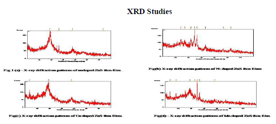
Fig.1 (a) – Fig.1 (d) shows the x-ray diffraction pattern of undoped and Mn/Ni/Cu doped ZnS thin films grown by spray pyrolysis technique. The diffraction pattern arising from the film has a single intense peak at ~ 29? due to the zinc blende (111) reflection. For Mn/Ni/Cu doped ZnS thin films , the peaks are at around 29?, 29.6?, 28.7? respectively. Additional x-ray diffraction peaks have been found to correspond to (200),(220) and (311) planes of the pure ZnS cubic phase(JCPDS 05-0566). The lattice constant a, is calculated from the peak position and is determined to be a=5.4060 A?. This indicates that the crystallites in the film have a single preferred orientation (111) and the zinc blende (111) plane was parallel to the substrate surface. This was expected since the cubic (111) lattice planes has the lowest surface energy [20]. In general, for a ZnS crystal, the zinc blende structural phase is stable at low temperature and the wurtzite structural phase is stable at temperature higher than 10230 C [21]. According to Scherrer formula, D = 0.94λ / βcosθ, Where D is the grain diameter, λ is the wavelength of the x-ray, β is the full width half maximum of the diffraction peak expressed in radians and θ is the Bragg diffraction angle. Using this expression, one can calculate the grain size for undoped and Mn/Ni/Cu doped ZnS thin films. The magnitude of the crystallite size does not change significantly with Mn/Cu doping in the ZnS thin films. The grain size values are on the order of 8 nm in all cases. The grain size increases on Ni doping and is of the order of 57 nm. Since the ionic radius of Ni2+ (0.69 A0 ) is smaller than that of Zn2+ (0.74 A0), it can be inferred that nickel ions might insert into the structure of ZnS and located at interstices or occupied some of the lattice sites of ZnS. From the x-ray diffraction studies, the following values are calculated using the corresponding formulas, and tabulated in the below table.
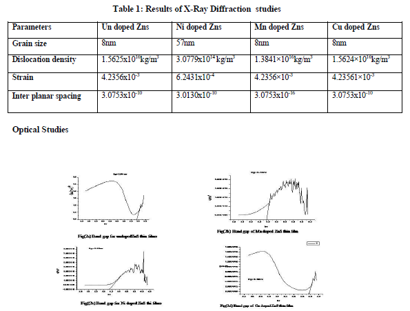
To study the optical properties of the thin films, the optical absorption spectra of the film is recorded in the wavelength range 300-1100 nm from which the absorption coefficient, refractive index, extinction coefficient, reflectance, optical conductivity and the band gap are calculated from the respective formulas and plotted(fig 2). The determined values are tabulated in table 2. To quantify the optical band gap(Eg) of films, the following formula is employed in the high absorbance region of the transmittance spectra,
(αhγ)n = A(hγ - Eg)
Where α is the absorption coefficient, A is a constant which is independent of photon energy and hγ is the photon energy, Eg is the optical band gap and n has numeric values (1/2 for allowed direct, 2 for allowed indirect, 3 for forbidden direct and 3/2 forbidden indirect optical transitions). In this work, direct bandgap was determined by plotting (αhγ)2 versus hγ curves respectively, with the extrapolation of linear region to low energies.The following values relating to optical properties are calculated using the corresponding formulas and are tabulated.
The crystallographic structure of doped Ni/Cu/Mn may result in a change of electronic structure, which enables the absorption edge to shift towards longer wavelengths after the addition of Ni/Cu/Mn. The absorption edge shifting towards visible region explained the yellowish colour for the Ni doped ZnS thin films. The red shift in the absorption spectra may be due to larger grain size. The bandgap value of Ni/Mn doped ZnS thin films decreases thus makes it to use it in the visible region. The bandgap value of Cu doped ZnS thin films does not change appreciably.
Thickness Measurements
Thickness is one of the most important thin film parameter since it largely determines the properties of the films. Any physical quantity related to film thickness can in principle be used to measure film thickness. Methods of monitoring thickness can be categorized as mechanical, electrical, magnetic, radiation, optical, mass diffraction methods etc., of which mass difference methods are most commonly used for measuring thickness of chemically deposited. Electrical methods of film thickness measurements involve film resistance method, capacitance monitor method and ionization method. Important optical methods are photometric, ellipsometric, spectrometer beam interferometer, including fizeau, FECO and Michelson beam interferometer and polarization interferometer methods. Stylus methods and sectioning are important mechanical methods for thickness determination. Two important mass methods for film thickness measurements are microbalance (gravimetric) method and crystal oscillator methods. In crystal oscillator method thickness measurement depends on the oscillation of quartz crystal when excites and the frequency of its oscillation depend on thickness change in frequency is due to the change in mass due to the deposition of a film on the quartz surface. For our study the thickness of the samples are measured with the help of Pyroheliometer. The calibration is carried out at the room temperature. In our study, the thickness of the undoped ZnS and Ni,Cu and Mn doped ZnS thin films are 853nm, 1.5μm, 53nm and 279nm respectively.
Scanning Electron Microscope Studies
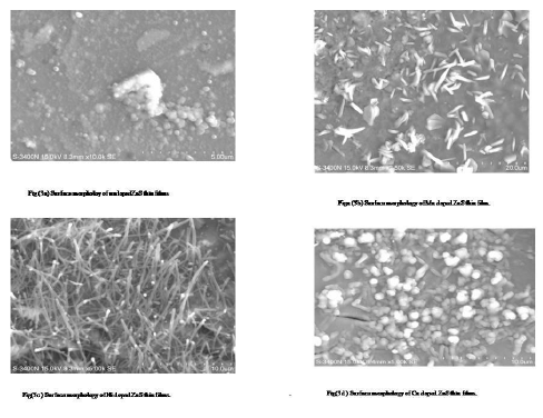
Figure (3a-d) shows that the surface of the undoped ZnS thin film is composed of clusters and few particles are found in some ware of cubic and hexagonal shaped nano crystals different dimensions and sizes. The surface of the Ni/Mn doped ZnS film is composed of the rods and sticks shaped nano crystals of different dimensions and sizes. The surface of the Cu doped ZnS film is composed of the small clusters and small rods. It should be noted that the average D values deduced from the scherrer formula are much lower than the sizes observable in the scanning electron microscope pictures. However, grains in the sizes less than a 100nm are also evident in the micrographs. The observed discrepancy can be probably due to the non spherical geometry of the nano crystallities. Infact, it is anticipated in the case of nano crystalline thin films that the domains have a tendancy to increase its size near the film surface, thus scanning electron microscope images representing the surface features of the film give the maximum possible size of the grains. On the other hand, the D values calculated using the x-ray diffraction data is thickness averaged magnitude, which usually dominated by the smallest crystallities. Similar discrepancy has been reported for various thin films. Grain sizes of these images are not homogeneously distributed as seen from this figure. Larger clusters of about 360nm and 650nm in size are formed; the clusters themselves are aggregate of grains. The apparent smaller size of ZnS grain and clusters in the thin films compared to that of the precipitate may be attributed to the geometric restriction in the aggregation process in the case of the film growth and that the smaller grains or clusters have high energy surface enough to stick to the surface of the substrate, due to this reason, the boundaries can’t be seen in the distinguished manner. It is good looking to note that the particles are regular and are of uniform sized distribution of about some nanometers. The morphological characterization revealed that the deposition temperature has an important role on the growth mechanism of both the thin films, so that with increasing temperature, the size of the building units(grains and clusters) of the films increases. It is to note that x-ray diffraction analysis reaveals the fact that grains themselves must be coalescene of nanocrystals of about 4-12 nm in the size as given in table.
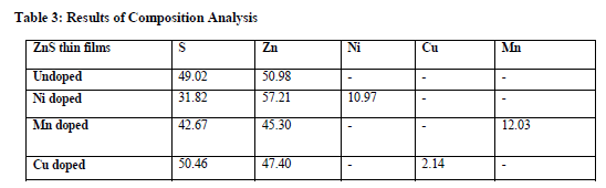
Composition Analysis [EDAX]
Chemical composition of undoped and Ni doped ZnS thin films was analyzed by Energy Dispersive X-Ray Analysis[EDAX]. Composition Analysis conforms the presence of Zn and S in Undoped ZnS thin films and also conforms the presence of Ni/Cu/Mn in the doped ZnS thinfilms. The atomic ratio(x) of Ni to ZnS determined from the relation, X= [(Ni/Mn/Cu)/(ZnS+(Ni/Mn/Cu))] to be x=0.1% for Ni/Mn and x=0.02% for Cu. Energy Dispersive X-Ray analysis shows how much amount of Ni atom has really entered into the ZnS thin films. Both atomic percentage(at%) and weight percentage(wt%) shown in the table proves the ratio of Ni/Mn/Cu dopant in the film. Therefore composition analysis conforms the incorporation of Ni element in the film. The composition of the pure ZnS films there is found to be more or less the same as doped ZnS and there was no significant variation in the composition.
CONCLUSION
Thin films of undoped and Ni/Mn/Cu doped ZnS are successfully prepared on glass substrates using spray pyrolysis technique. The films are characterized by means of scanning electron microscopy, x-ray diffraction, ultraviolet visible spectroscopy, composition analysis(energy dispersive x-ray analysis) and thickness measurements. x-ray diffraction studies show that ZnS films grown on glass preferentially orientation along the (111) direction. scanning electron microscope images confirm the formation of uniform grains for all samples. It has been established that the addition of Ni/Mn/Cu affects the growth mechanisms of films, the crystallographic structure and the absorption spectra. In the case of undoped ZnS thin film, sphere, hexagonal like branches are found, with the cubic structure have been absorbed by scanning electron microscope and x-ray diffraction. The composition analysis confirms the presence of Ni/Mn/Cu, Zn and S. The grain size is found to be 8nm and 57nm for undoped and Ni doped thin films and remained unchanged on doping with Cu/Mn, from x-ray diffraction analysis. The band gap is found to be 3.94eV and 3.23eV, 3.18eV, 3.96eV for undoped and Ni,Mn,Cu doped thin films respectively as calculated from UV studies.
References:
- Ogura .T, Mikami . A, Tanaka .K, Taniguchi.K, Yoshida . M, Nakajima.S Appl. Phys. Lett. 48 (1986) 1570.
- Lewis JS, Davidson MR, Holloway PH, J Appl. Phys. 92 (2002) 6646.
- Monroy E, Omnes F, Semicond. Sci. Technol. 18(2003) R33..
- Rusu M, Eisele W, Wurz R, Emnaoui A, Chi M,Lux-Steiner, Neisen TP, Karg F, J. Phys. Chem. Solids. 64 (1974) 165.
- Murray.H, Tosser.A, Thin Solid Films. 24 (1974)165.
- Zhang.Z.Z, Shen D.Z, Zhang J.Y, Shan C.X, Lu.Y.U, Liu, Y.C, Li B.H, Zhao.D.X, Yao.B, Fan X.W, Thin Solid Films. 513 (2006) 114.
- Bacaksiz.E, Dzhafarov. T.D, Novruzov.V.D, Ozturk.K,Tomakin.m, Kucukomeroglu,T, Altunbas.M, Yanmaz.E, Abay.B, Phys. Status Solidi. A.Appl.Res. 201 (2004) 2948.
- Zhai.R, Wang.S, Xu.H, Wang.H, Yan.H, Mater.Lett. 59 (2005(12)) 1497..
- Bhosale.C.H, Kambale.A., Kokate.A.V, Rajpure.K.Y, Mater. Sci. Eng.,B 122 (2005) 67.
- Podesta.A, Armani.N, Salviati,G. Romeo.N, Bosio.A, Prato.M, Thin Solid Films 448 (2006) 511-512.
- Rodriguez-Baez.J, Maldonada.A, Torres-Delgado.G, Castanedo-Perez.R, De la.M, Olvera.L, Mater. Lett. 60 (2006) 1594.
- Aukkaravittayapun.S, Wongtida.N, Kaseewatin.T, Charochkul.S, Unnanon.K, Chindaudom.P, Thin Solid Films. 496 (2006) 117.
- Cheng K.W, Huang C.M, G.T.Pan,Chen.P.C,Lee.T.C,Yang.T.C.K,Mater.Chem.Phys. 108(2008) 16 Erat.S, Metin.H, Ari.M, Mater.Chem.Phys. 111(2008) 114.
- Geng.B.Y, Zhang.L.D, Wang.G.Z,Xie.T, Zhang.Y.G, Meng.G.W, Appl.Phys.Lett. 84(2004) 2157
- Khosravi.A.A, Kundu.M, Jatwa.L, Deshpande.S.K, Bhagawat.U.A, Sastry.M, Kulkarani.S.K, Appl. Phys. Lett. 67(1995) 2702. .
- Lee.S,Song.D, Kim.D,Lee.J, Kim.S, Park.I.Y, Choi.Y.D, Mater. Lett. 58(2004) 342.
- Yang.P, Lu.M, Xu.D,Yuan.D,Chang.J,Zhou.G,Pan.M, Appl. Phys. A 74 (2002) 257.
- Huang.C.M, Chen.L, Pan G.T, Yang T.C.K, Chang W.S, Cheng K.W, Mater. Chem. Phys., 117 (2009) 156.
- Wright.K, Watson.G.W, Parker.S.C, Vaughan.D.J, J. Am. Mineral 83 (1998) 14.
- Hiramatsu.H, Ohta.H, Hirano.M, Hosono.H, Solid State Commun. 124 (2002) 411
|
 IJCRR
IJCRR 


 This work is licensed under a Creative Commons Attribution-NonCommercial 4.0 International License