IJCRR - 9(24), December, 2017
Pages: 01-05
Date of Publication: 26-Dec-2017
Print Article
Download XML Download PDF
Electrical Measurements on Cadmium Selenite Nano Composites
Author: Nima Jessieba Daniel, N. Thangaraj, D. M. Suresh, N. Joseph John
Category: General Sciences
Abstract:By simple microwave irradiated solvothermal process using microwave oven Cadmium Selenite (CdSeO3) nanoparticles were prepared. Cadmium acetate and Sodium selenite were used as precursors in the molar ratio 1:3. The powder XRD result shows that particles are purely crystallized in hexagonal phase with the broadening of diffraction peaks attributed to nanoscale size of the particles. The dielectric measurements were carried in two frequencies for temperatures ranging from 40 to 150oC. The present study indicates that the polarization mechanism in the nano particles considered is mainly contributed by space charge polarization. It can be understood that the space charge contribution plays an important role in the charge transport and polarizability in all the systems considered in the present study. The dielectric constant, dielectric loss, AC conductivity and DC conductivity increases with increase in temperature.
Keywords: Nanoparticles, Microwave, AC conductivity, DC conductivity, Dielectric constant, Dielectric loss
DOI: 10.7324/IJCRR.2017.9241
Full Text:
Introduction
Semiconductor nano crystals have attracted impressive attention, because of their novel optical and electronic properties [1]. Varying the size of the particle and changes in the degree of confinement of the electron and affects the electronic structure of the solid in particular band edges, which are tunable with particle size. One of the most important II – VI group semiconductors and nano crystalline Wurtzite structured Cadmium Selenide has attracted great interest in their various promising optoelectronic applications owing to its excellent optical conductivity such as photoelectron chemicals, photo-conductors , thin film transistor [2-4]. Blue shift in the band gap of this material, with decreasing grain size has led to many applied investigations. Many strategies have been utilized to prepare 1-D nano structural materials, where wet chemical method is considered as a practical and effective method for the synthesis of 1-D nano materials because it is more convenient and facile to be compared with most physical methods and need little expensive equipment by which CdSe nanorods, nanowires and nano tubes have been prepared successfully.
CdSe has been considered in many applications such as optoelectronic devices [5], light sensors [6], biological labels [7], chemical libraries [8], etc. The nanopowder of CdSe provides excellent and unique properties which depend upon the shape and size of the nanostructures [8-12]. Various methods such as hydrothermal, sol–gel approach, surfactant-assisted approach, etc. had been utilized for the synthesis of nanoparticles [13,14]. Synthesis, structural, and optical properties of CdSe nanoparticles have been reported [15]. In the present study, the main focus is on the electrical properties of pellets of nanoparticles of CdSeO3 at different temperatures. The temperature dependence of dielectric constant, dielectric loss ac conductivity and dc conductivity was also investigated.
Experimental
The chemicals such as cadmium acetate dehydrate and sodium selinite were used as precursor materials to prepare CdSeO3 nano particles. Cadmium acetate dihydrate and sodium selinite in 1:3 ratio were dissolved in Ethylene glycol solvent and water and stirred well using a magnetic stirrer and this solution mixture is kept in a microwave oven till the solvent evaporates completely, then the colloidal precipitate is filtered and washed by water and acetone several times. The precipitate thus formed is collected and dried.
AC conductivity measurements
The prepared cadmium selenite samples were palletized using a hydraulic press (with a pressure of about 5 tons) and used for the AC electrical measurements. The flat surfaces of the cylindrical pellets were coated with good quality graphite to obtain a good conductive surface layer. Using a traveling microscope the dimensions of the pellets were measured. The capacitance (Cc ) and the dielectric loss factor (tan δ) were measured using the conventional parallel plate capacitor method [16-19] using an LCR meter (APLAB MODEL 4912) for all the samples with two frequencies 100 Hz and 1 kHz at various temperatures in the range 30 – 150°C. The observations were made while cooling the sample. The temperature was controlled to an accuracy of ±1°C. Air capacitance (Ca) was also measured for the thickness equal to that of the pellet. The area of the pellet in contact with the electrode was same as that of the electrode. The air capacitance was measured only at room temperature because the variation of air capacitance with temperature was found to be negligible. The dielectric constant of the pellet sample was calculated using the relation,
εr = Cc / Ca.
where Cc is the capacitance of the crystal and Ca is the capacitance of the air medium of the same dimension as the crystal. As the crystal area was smaller than the plate area of the cell, parallel capacitance of the portion of the cell not filled with the crystal was taken into account and, consequently, the above equation becomes

where Ccrys is the capacitance with crystal (including air), Cair is the capacitance of air, Acrys is the area of the crystal touching the electrode and Aair is the area of the electrode. From these measurements, er and tan δ (dielectric loss factor) are available for the evaluation of AC conductivity.
The AC electrical conductivity (σac) was calculated using the relation,
σac = ε 0 εr ω tan δ.
Here, ε0 is the permittivity of free space (8.85 x 10⁻¹² C2 N-1 m-2) and ω is the angular frequency (ω= 2πf, where f is the frequency).
DC Conductivity Measurements
The DC electrical conductivity measurements were carried out to an accuracy of ±3% using the conventional two-probe (parallel plate capacitor) technique at various temperatures in the range 40–150 ºC [20-22]. The sample was prepared as done for the AC conductivity measurement. The resistance of the sample was measured using a million megohmmeter. The observations were made while cooling the sample. Temperature was controlled to an accuracy of ±1 ºC. The dimensions of the sample were measured using a traveling microscope (least count = 0.001 cm). The DC conductivity, σdc, of the crystal was calculated using the relation
σdc = d/(RA)
where R is the measured resistance, d is the thickness of the sample, and A is the area of the face in contact with the electrode.
Results and Discussion:
Powder XRD analysis
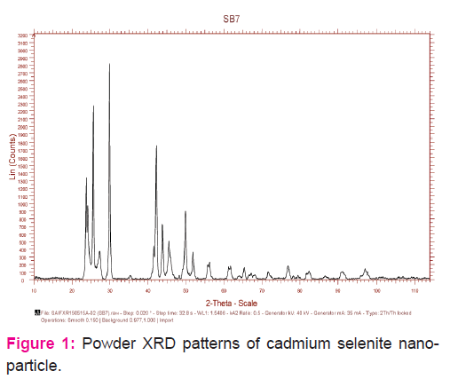
The powder XRD pattern for the as prepared sample was done using Bruker AXS D8 Advance Diffractometer with monochromatic Cu (λ=1.5406 A0) radiation. The XRD pattern of as prepared CdSe nanoparticles are shown in Fig.1. The diffraction peaks indicates the nanocrystalline nature. The intensity of the peaks shows that the CdSe nanoparticles are highly crystalline. The diffracted peaks (100),(002), (101),(102),(110), (103), (112),(004), (202), (210), (211), (105) and (300)are corresponding to Hexagonal phase with Wurtzite structure which are in very good agreement with hexagonal (P63mc) structure in (Join Committee on Powder Diffraction Standards) JCPDS CAS No. 08-0459 .The corresponding lattice constants are a = 4.299 Å and c =7.010 Å. The size of the nanocrystallites was estimated using the Debye-Scherrer formula (Sagirani et al. 2015)
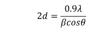
where, A is coherence length, β is the full-widths-at-half maximum (FWHM) of the diffraction peak, λ (1.5418 Å) is the wavelength of X-ray radiation, and θ is the angle of diffraction. From different θ values, the calculated average particle size is about 28 nm.
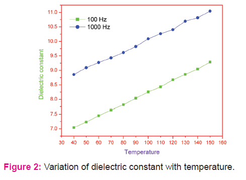
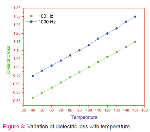
The dielectric parameters viz. εr, tan δ and σac observed are shown in Figures 2-4. All the parameters increase with increase in temperature. The dielectric constant is attributed to four types of polarization which are space charge, dipolar, ionic and electronic [23]. At lower frequencies at which all four types of polarizations contribute, the rapid increase in dielectric constant is mainly due to space charge and dielectric polarizations, which are strongly temperature dependent [24]. In the case of space charge polarization which is due to the accumulation of charges at the grain boundary, an increase in polarization results as more and more charges accumulate at the grain boundary with the increase in temperature. Beyond a certain temperature, the charges acquire adequate thermal energy to overcome the resistive barrier at the grain boundary and conduction takes place resulting in decreasing of polarization. This interfacial polarization occurs up to frequency of 1 kHz with possibly some contribution from the dipolar polarization also as the temperature increases. The grain size observed for the system considered in the present study is significantly small (not more than 26 nm). So, it can be understood that the polarization mechanism is mainly contributed by the space charge polarization[25-29].
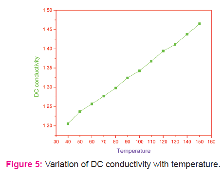
The observed DC electrical conductivities of cadmium nanocomposite are shown in Fig 5. Nanoparticles lie between the infinite solid state and molecule. The electrical resistivity of nanocrystalline material is higher than that of both conventional coarse grained polycrystalline material alloys. The magnitude of electrical resistivity and hence the conductivity in composites can be changed by altering the size of the electrically conducting component. The σac values observed in the present study are very small. When the grain size is smaller than the electron mean free path, grain boundary scattering dominates and hence electrical resistivity is increased [30]. Thus the space charge contribution plays an important role in the charge transport process and polarizability for the system considered in the present study.

Conclusion
Semiconductor nanoparticles of cadmium selenite were successfully prepared bysimple microwave assisted solvothermal process. The powder XRD result shows that particles are purely crystallized in hexagonal phase with the broadening of diffraction peaks attributed to nanoscale size of the particles. The dielectric parameters, viz. dielectric constant (εr), dielectric loss (tan δ) and AC electrical conductivity (σac) and DC conductivity (σdc) measurements were also carried out at various temperatures in the range 40-150ºC and these electrical parameters are found to increase with the increase in temperature.
References:
[1] D. Mohanta, G.A. Ahmed, F. Singh, D. K. Avasthi and A. Choud-hury, “Properties of MeV oxygen ion irradiated Zns:Mn nanoparticle and exploitation in nanophotonics”, Journal of nanoparticle Research, vol. 8, pp. 645-652, 2006.
[2] S. J. Lade, M. D. Uplane and C. D. Lokhande, “Photoelectro chemical properties of CdX (X=S, Se, Te) films electrodeposited from aqueous and non aqueous baths”, Materials chemistry and physics, vol. 68, no.1, pp. 36-41,2001.
[3] M. T. S. Nair, P. K. Nair, R. A. Zingaro, and E. A. Meyers, “Enhancement of Photosensitivity in Chemically Deposited CdSe Thin Films by Air Annealing”, Journal of Applied Physics, vol. 74, no.3, pp. 1879-1884,1993.
[4] Ganganagappa, Nagaraju and Gujjarahalli Thimmanna Chandrap-pa, “Surfactant assisted hydrothermal synthesis of CdSe nanostructural materials” J. Mater. Sci. Technol., vol. 28, no. 6, pp. 495-499, 2012.
[5]. Nazzal AY, Qu L, Peng X, Xiao M (2003) Photoactivated CdSe nanocrystals as nanosensors for gases. Nano Lett 3:819–822
[6]. Bruchez M, Moronne M, Gin P, Weiss S, Alivisatos AP (1998)Semiconductor nanocrystals as fluorescent biological labels. Science 281:2013–2016
[7]. Colvin VL, Schlamp MC, Alivisatos AP (1994) Light-emitting diodes made from cadmium selenide nanocrystals and a semiconducting polymer. Nature 370:354–357
[8]. Gaponik N, Radtchenko IL, Sukhorukov GB, Rogach AL (2002) Toward encoding combinational libraries: charge-driven microencapsulation of semiconductor nanocrystals luminescing in the visible and near IR. Adv Mater 12:879–882
[9]. Haram SK, Quinn BM, Bard AJ (2001) Electrochemistry of CdS nanoparticles: a correlation between optical and electrochemical band gaps. J Am Chem Soc 123:8860–8861
[10]. Wang ZL, Kong XY, Ding Y, Gao P, Hughes WL, Yang R, Zhang Y (2004) Semiconducting and piezoelectric oxide nanostructures induced by polar surfaces. Adv Funct Mater 14:943–956
[11]. Hench, L, C. and West, J, K. Principles of Electronic Ceramics 1990, [John Wiley and Sons, NewYork] ISBN10 0471618217
[12] Peng XG, Manna L, Yang WD, Wickham J, Scher E, Kadavanich A, Alivisatos AP (2000) Shape control of CdSe nanocrystals. Nature 404:59–61
[13]. Tang KB, Qian YT, Zeng JH, Yang XG (2003) Solvothermal route to semiconductor nanowires. Adv Mater 15:448–450
[14] Busbee BD, Obare SO, Murphy CJ (2003) An improved synthesis of high-aspect-ratio gold nanorods. Adv Mater 15:414–416
[15]. Dwivedi DK, Kumar V, Dubey M, Pathak HP (2011) Structural, electrical and optical investigations of CdSe nanoparticles. Chalcogenide Lett 8:521–527
[16]. Joseph John, Selvarajan P, Benita Jeba Silviya S., Mahadevan C. K, Growth and
Characterization of Disodium Hydrogen Orthophosphate (DSHP) Single Crystals, Materials and
Manufacturing Processes, 22:3, 379 – 383.
[17]. Joseph John, N. Mahadevan, C, K. Studies on NaCl Added ADP Single Crystals. Materials and Manufacturing Processes 2008, 23, 809-815.
[18] Joseph John N, Selvarajan P, Mahadevan C K, Growth, Structural, Optical, Mechanical and Dielectric Characterization of Diammonium Hydrogen Phosphate (DAHP) single Crystals, Journal of Minerals and Material characterization and Engineering, 10, 15, 1379 (2011).
[19] Joseph John N. “Growth and Studies on Ferroelectric Material L-proline doped TGS single crystals for IR detectors” , Int. J. Current Sci. 8,11, 2016, 41068-41074
[20] Jayaprakash Manoharan J A, Joseph John N , Andavan P, Effect of amino acid doping on the dielectric properties of triglycine sulphate (TGS) single crystals , Ind. J. of Sci. and Tech., 4,6, 688, (2011).
[21] Jayaprakash Manoharan A J, Joseph John N, Andavan P, Journal of Experimental Sciences, 2(2) (2011), 33.
[22] Sivaka P, Joseph John N, Perumal S, Int. Journal of Engineering Research and Applications, 4, 7 (2014), 145.
[23] Sivaka P, Joseph John N., Perumal S, Int. res. J. Eng. And Tech., 3, 2 (2016), 1273.
[24]. Joseph John N. “Dielectric properties of ferroelectric L-proline triglycine sulphate (LPTGS) crystal” Int. J. Innov. Sci. and Res. 5,11, 2016, 890-893
[25]. Ajin Sundar S., Joseph John N. “ Dielectric properties of Mn doped ZnO nanostructures”, Int. J. of Eng. and App. Sci.3, 3, 2016, 26-29.
[26]. Ajin Sundar S., Joseph John N., Investigation on the effect of Mn on structural and optical properties of ZnO nanoparticles, Int. J. current Research, 2016, 8, 4, 29398-29402
[27]. Ajin Sundar S. , Joseph John N., Synthesis and studies on structural and optical properties of zinc oxide and manganese doped zinc oxide nanoparticles, Nano systems : Physics, Chemistry and Mathematics , 2016, 7(6)P.1-7
[28]. Ajin Sundar S., Joseph John N., “Carbon dot – Graphene oxide - Zinc oxide nanocomplex: Synthesis, characterization and properties” Materials Science-Poland, In press
[29]. Ajin Sundar S., Joseph John N., “Synthesis, Structural, Optical and Dielectric Studies on Carbon dot-Zinc oxide (CDZO) nanocomplexes” – Int. J. nanoscience, 2017, 16, 3, 1750021 – 1750030
[30] Sagi Rani C., Athira P., Joseph John N. “Investigations on tri manganese tetra oxide nano particles prepared by thermal decomposition “, Nanosystems: Physics, Chemistry, Mathematics, 2016, 7 (4), P. 0–2
|
 IJCRR
IJCRR 


 This work is licensed under a Creative Commons Attribution-NonCommercial 4.0 International License