IJCRR - 3(7), July, 2011
Pages: 24-36
Print Article
Download XML Download PDF
EFFECT OF THICKNESS AND ANNEALING TEMPERATURES ON STRUCTURAL AND MORPHOLOGICAL PROPERTIES OF (SB2S3)1-X (BI2S3)X THIN FILMS
Author: Jessy Mathew N., Rachel Oommen, C. Sanjeeviraja , Usha Rajalakshmi P
Category: General Sciences
Abstract:(Sb2S3)1-x (Bi2S3)x (with x= 0.03, 0.05, 0.1) thin films were prepared on chemically well cleaned glass substrates by thermal evaporation technique for two thickness. The orthorhombic crystal structure of the (Sb2S3)1-x (Bi2S3)x powder samples and thin films have been found out from XRD powder data and confirms the transition of films from amorphous to polycrystalline with thermal treatment at 523K. Also lattice parameters, crystallite sizes and interplanar spacings for the newly prepared ternary compounds (Sb-Bi-S) have been calculated. The XPS spectra were carried out to identify the surface compositions. The elemental percentage in each compound was verified by EDAX. Increase of crystallite size with thickness and temperature was proved by
XRD and the influences of thickness and annealing temperature on roughness and grain size was observed from AFM measurements.
Keywords: Thermal evaporation technique, Ternary compounds, Amorphous, Polycrystalline, Orthorhombic crystal structure
Full Text:
1. INTRODUCTION
The ternary semiconductor compounds in thin film form have become the focus of attention because of their important physical and chemical properties since these properties could be changed by varying the annealing temperature and thickness. Thin films of semiconductor chalcogenides of the chemical formula m2 V-B - n3 VI-B basically have the structure of antimony sulphide which are most important materials for the applications in photosensitivity, photoconductivity and thermoelectric power1 . Antimony sulphide and Bismuth sulphide are layer structured direct band gap semiconductors with orthorhombic crystal structure have been received considerable interest because of their structural, morphological, optical and electrical properties which allow their wide use in many devices. A number of methods have been used for the preparation of V-VI compound thin films by the thin film investigators like, N.S. Yesugade et al.2 prepared Sb2S3 and Bi2S3 thin films by electrodeposition technique, Gang Xie et al.3 synthesized M2S3 (M = Sb, Bi) via a hydrothermal treatment, Pawan Kumar et al.4 prepared Bi2S3 thin films by spray pyrolysis technique, Siham Mahmoud et al.5 produced thin films of Bi2S3 by thermal evaporation technique, I.K. El Zawawi et al.6 prepared Sb2S3 thin films by thermal vacuum evaporation technique, I. Grozdanov et al.7 fabricated thin films of Sb2S3 by chemical deposition technique etc. Pawar et al.2 obtained Bi2S3, Sb2S3 and As2S3 films by a solution-gas interface technique. This paper reports the investigations on the effect of thickness and annealing temperature on the structural and morphological properties of thermally evaporated (Sb2S3)1-x (Bi2S3)x (with x= 0.03, 0.05, 0.1) thin films from newly prepared powder samples. Characterizations were done by means of Energy Dispersive X-ray Analysis (EDAX), X-ray Diffraction (XRD) technique, X-ray Photoelectron Spectroscopy (XPS) and Atomic Force Microscopic (AFM) analysis. To the best of our knowledge nobody has performed the work on the preparation and characterization of (Bi2S3)x doped (Sb2S3)1-x (with x= 0.03, 0.05, 0.1) thin films from the freshly prepared powder samples and thermal vacuum evaporation technique as the method of deposition.
2. MATERIALS AND METHODS
Bulk thin film samples of (Sb2S3)1-x (Bi2S3)x (with x= 0.03, 0.05, 0.1) were prepared from powder materials of Sb2S3 and Bi2S3 (99.999% purity, Sigma-aldrich) on chemically cleaned glass substrates by thermal vacuum evaporation technique. The conventional thermal evaporation method is being widely used for the growth of binary and ternary compounds because of its simplicity and this method supports high quality and pure films for thin film applications. For a particular composition, the constituent compounds Sb2S3 and Bi2S3 were weighed and grinded for several hours and sintered. The newly prepared powder samples were used as the source material. During deposition the precleaned substrates were placed in a rotative sample-holder to get uniformly coated films. Deposition rate and film thickness were controlled during deposition by quartz oscillator thickness monitor. The substrate temperature was maintained at 300K during the deposition. The deposition chamber was evacuated to a residual pressure of about 10-5 torr. The elemental compositions of the prepared powder and thin films were determined using an Energy Dispersive X-ray Analysis (EDAX) (model: INCA Oxford) based on SEM images. X-ray Diffractograms of the prepared material and the investigated films of as-deposited and annealed (473K, 523K) samples were carried out by using an X-ray Diffractometer (XRD) (model: D8 Advance XRD) with CuKα (λ=1.5406Å) radiation. To analyse the surface compositions and purity, the x-ray photoelectron spectroscopy (XPS) data were recorded with the specimen mounted on a specially designed sample holder8 using an AlKalpha laboratory x-ray source that was operated at 150 watts and an electron energy analyser with five channeltrons from Specs GmbH, Germany. The data were recorded with 20 eV pass energy with 1 eV energy resolution. The chamber base pressure was 6×10-11 mbar. Surface morphological studies were done before and after heat treatment by means of Atomic Force Microscope (AFM) and surface roughness and grain size were estimated.
3. RESULTS
3.1. Compositional analysis
Fig. 1 shows the Energy Dispersive X-ray Analysis (EDAX) spectra for the powder samples and the corresponding thin films of (Sb2S3)1-x(Bi2S3)x, with x= 0.03, 0.05, 0.1. The calculated and observed percentages of the elements in different compositions from EDAX analysis are shown in table 1 and are in good agreement each other. (Figure 1, Table 1)
3.2. Structural analysis
The X-ray diffractograms of the as-deposited, annealed (473K, 523K) thin films and powder samples of (Sb2S3)1-x(Bi2S3)x with x= 0.03, 0.05, 0.1 are shown in figures (2-13). It is clear from figs. (2-7) the as-deposited films and the films annealed at 473K are amorphous in nature9-10 . As reported by F. Perales et al.11, it was proved that the effect of annealing at 473K cannot change the amorphous nature. Thin films have been annealed for 1hr at 523K to investigate the effect of higher annealing temperature, and the growth of polycrystalline from amorphous phase. This observation is in agreement with the results of M. S. Droichi et al.12 for Sb2S3 and Mahmoud et al.10 for Bi2S3 thin films.
(Fig. 2 Fig. 3)
(Fig. 4 Fig. 5)
(Fig. 6 Fig. 7)
From figs. (8-10), it is clear that the increase of thermal treatment improves crystallinity of SbBi-S films with orthorhombic structure. The Xray diffractograms of (Sb2S3)1-x(Bi2S3)x with x= 0.03, 0.05, 0.1 for powder samples are shown in figures (11-13).
(Fig.8 Fig. 9)
The orthorhombic crystal structure of these compounds, both in powder and thin film forms, with cell parameters have been found out from XRD powder data. The position of peaks appeared in the diffractograms of the powder sample lie very near to those listed in the PDF for Sb2S3 (PDF 42-1393) and Bi2S3 (PDF 17- 0320). The estimated values of the lattice parameters lie close to the reported values of Sb2S3 and Bi2S3 11, 13 .
(Fig. 10 Fig.11)
(Fig.12 Fig.13)
The crystallite size D estimated using the Sherrer‘s formula14:
where K is the shape factor (0.94), β is the full width at half maximum (FWHM) of the diffraction expressed in radians. The estimated lattice parameters for both powder and thin films and crystallite size for the annealed film samples of (Sb2S3)1-x(Bi2S3)x with x= 0.03, 0.05, 0.1 of different thickness are recorded in table 2. Using Bragg‘s relation14, the interplanar spacing dhkl was also calculated from powder diffraction data:
where λ is the X-ray wavelength, n is the order number and θ is the Bragg‘s angle. Table 3 shows the calculated dhkl values of Sb-Bi-S compound in comparison with the standard powders of Sb2S3 (JCPDS card No. 42-1393) and Bi2S3 (JCPDS card No. 17-0320) and in agreement with the recorded values by A.A. ElShazly et al.15 and Siham Mahmoud et al.5 . The surface composition and purity of the asdeposited (Sb2S3)0.95 (Bi2S3)0.05 thin film were studied by XPS analysis and the core level spectra are given in figs. (14-16). The photoelectron spectra of the Sb(3d3/2), Bi(4d5/2) and S(2p) show the peaks at the binding energy 537.61eV, 440.01eV and 162. 21eV respectively.
(Fig. 14)
(Table 2)
3.3 Morphological analysis
The surface topographical images for Sb-Bi-S thin films, deposited at room temperature and annealed at 523K for 1 hr, of film thickness 900nm and 1200nm recorded from atomic force microscope (AFM) are shown in fig.15. This measurements have been taken for films from the compound with x=0.05. The measured grain size and RMS roughness from AFM images for thickness 900nm and 1200nm are given in table 4. It is observed from the AFM images that the average grain size and roughness increase with increasing thickness and temperature16 . (Fig. 15)
(Table 3)
(Table 4)
3. DISCUSSIONS
As the crystallization process proceeds with thickness at temperature 523K, the intensity of the (310) peak increases for x=0.03 compound, (120) peak increases for x=0.05 compound and (130) peak increases for x=0.1 compound, indicating further orientation of the film crystallites in these directions. And also, in all the three compounds, more peaks appeared in films of highest thickness (1200nm). Some peaks appeared, which are common to both Sb2S3 and Bi2S3 like, (120) and (250) for x=0.03, (120) and (240) for x=0.05, (120), (130), (240) and (250) for x=0.1. The calculated values of the lattice parameters for the three compounds lie close to the reported values of Sb2S3 and Bi2S3. The calculated interplanar spacing dhkl values of Sb-Bi-S compound lie close to the standard powders of Sb2S3 (JCPDS card No. 42-1393) and Bi2S3 (JCPDS card No. 17-0320). As K.Y. Rajpure et al.17 point out, annealing promotes fusion of small crystallites thus reducing the grain-boundary area, which leads to an increase in diffusion length due to decrease in scattering from boundaries. This leads to an increase in crystallite size of the particles. The crystallite size increases with: a) increasing film thickness and b) increasing annealing temperature16. The linear increase of surface area with the film thickness suggests that a porous film structure with its relatively large internal surface area accessible to the absorbing gas even in the lowest layaers of the film. 4.
CONCLUSIONS
The thermal evaporation technique has been used to prepare (Sb2S3)1-x(Bi2S3)x with x=0.03, 0.05, 0.1 thin films on glass substrate for two thickness. The measurements obtained from EDAX showed the elemental percentages of respective compounds. The orthorhombic crystal structure of all compounds with x=0.03, 0.05 and 0.1 and lattice parameters and the dependence of crystallite size on thickness were showed by X-ray Diffraction (XRD) measurements. The as-deposited amorphous thin films transformed to polycrystalline films during the thermal treatment at 523K. The XPS core level spectra of Sb(3d3/2), Bi(4d5/2) and S(2p) showed the peaks of corresponding binding energies. Dependence of grain size and RMS roughness on thickness and annealing temperature was proved by atomic force microscopic (AFM) photographs.
ACKNOWLEDGEMENT
The measurements have been taken in the UGCDAE Consortium for Scientific Research, Indore. The authors are much grateful to the supporting authorities, especially to Prof. Ajay Gupta- the centre Director of Indore. The corresponding author is also much grateful to the financial support given by DST- CURIE Project.
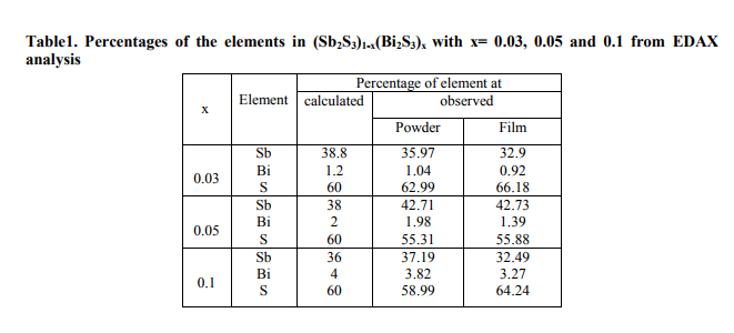
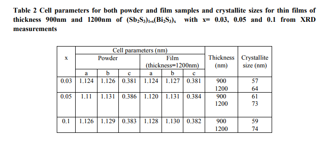
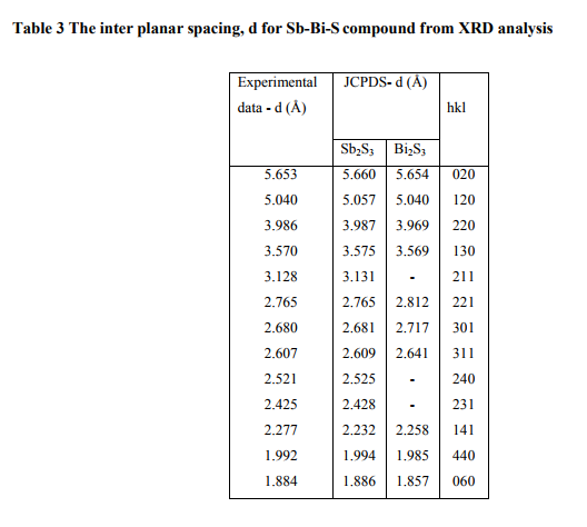
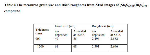
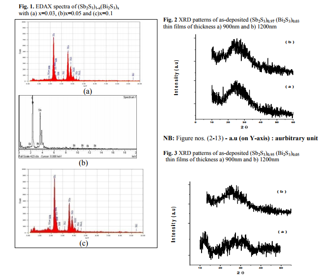
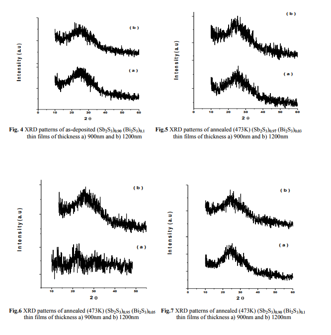
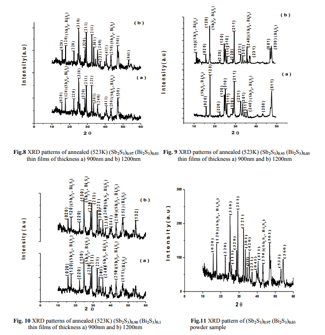
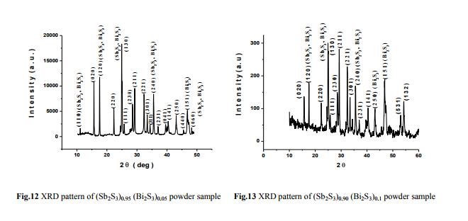
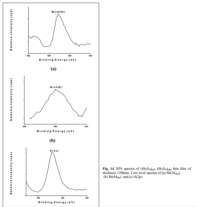
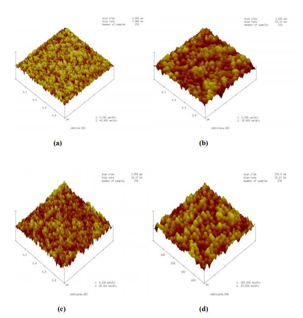
Fig.15 AFM images of the (Sb2S3)0.95(Bi2S3)0.5 thin films for thickness 900nm [as-deposited (a), annealed (b)] and for 1200nm [as-deposited (c), annealed (d)]
References:
1. Lokhande C D, Sankapal B R, Sartale S D, Pathan H M, Giersig M, Ganesan V. A novel method for the deposition of nanocrystalline Bi2Se3, Sb2Se3 and Bi2Se3- Sb2Se3 thin films - SILAR. Appl Surf Sci 2001; 182:413-7.
2. Yesugade N S, Lokhande C D, Bhosale C H. Structural and optical properties of electrodeposited Bi2S3, Sb2S3 and As2S3 thin films. Thin Solid films 1995; 263:145-9.
3. Gang Xie, Zheng-Ping Qiao, Ming-Hua Zeng, Xiao-Ming Chen, Sheng-Li Gao. A single-source approach to Bi2S3 and Sb2S3 nanorods via a Hydrothermal treatment. Crystal Growth and Design 2004; 4:513-6.
4. Pawan Kumar, Nidhi Jain, Agarwal R K. Effect of substrate temperature on optical properties of Bi2S3 chalcogenide thin films. Chalcogenide Letters 2010; 7:89-94.
5. Siham Mahmoud, Fouad Sharaf. Optical and electrical properties of Bismuth sulphide (Bi2S3) thin films prepared by thermal evaporation. Fizika A5 1996; 4:205-13.
6. El Zawawi I K, Abdel-Moez A, Terra F S, Mounir M. Substrate temperature effect on the optical and electrical properties of antimony trisulfide thin films. Thin Solid Films 1998; 324: 300-4.
7. Grozdanov I, Ristov M, Sinadinovski Gj, Mitreski M. Fabrication of amorphous Sb2S3 films by chemical deposition. J NonCryst Solids 1994; 175: 77-83.
8. Dhaka R S, Shukla A K, Maniraj M, D‘Souza S W, Nayak J, Barman S R. An ultrahigh vacuum compatible sample holder for studying complex metal surfaces. Rev Sci Instrum 2010; 81: 043907.
9. Tigau N, Rusu G I, Gheorghies C J. On the structural and optical properties of antimony trisulfide thin films. Optoelect Adv Mater 2002; 4: 943-8.
10. Mahmoud S, Eid A H, Omar H. Optical characteristics of bismuth sulphide (Bi2S3) thin films. Fizika A6 1997; 3:111-20.
11. Perales F, Lifante G, Agullo-Rueda F, de las Heras C. Optical and structural properties in the amorphous to polycrystalline transition in Sb2S3 thin films. J Phys D Appl Phys 2007; 40: 2440-4.
12. Droichi M S, Vaillant F, Bustarret E, Jousse D. Study of localized states in amorphous chalcogenide Sb2S3 films. J Non-Cryst Solids 1988; 101: 151-5.
13. Sheng-Yue Wang, You-Wei Du. Preparation of nanocrystalline bismuth sulphide thin films by asynchronous-pulse ultrasonic spray pyrolysis technique. J Cryst Growth 2002; 236:627–34.
14. Nicolae Tigau. Structural characterization and optical properties of annealed Sb2S3 thin films. Rom Journ Phys 2008; 53: 209-15.
15. El-Shazly A A, Sayem M A M, ElSamanoudy M M, Ammar A H, Assim E M. The effect of deposition rate and heat treatment on conduction and charge carrier transport mechanisms in Sb2S3 films. Appl Surf Sci 2002; 189: 129-37.
16. Kasturi L Chopra. Thin Film Phenomena. 2 nd ed. New York: McGraw-Hill; 1969.p.188, 183.
17. Rajpure K Y, Bhosale C H. Effect of composition on the structural, optical and electrical properties of sprayed Sb2S3 thin films prepared from non-aqueous medium. J Phys and Chem Solids 2000; 61:561-8.
|
 IJCRR
IJCRR 


 This work is licensed under a Creative Commons Attribution-NonCommercial 4.0 International License