IJCRR - 3(9), September, 2011
Pages: 114-121
Print Article
Download XML Download PDF
STRUCTURAL AND OPTICAL CHARACTERIZATION OF THERMALLY EVAPORATED BI2S3 THIN FILMS
Author: Usha Rajalakshmi P., Rachel Oommen, Jessy Mathew N.
Category: General Sciences
Abstract:Bismuth sulphide (Bi2S3) thin films are deposited on microscope glass slides by single source thermal evaporation technique. The properties of the films are analysed by X-ray diffraction, Raman spectroscopy, atomic force microscopy and UV-Vis. spectrophotometry. The effect of post deposition vacuum annealing and thickness on the properties of the films are investigated. The X-ray diffractograms revealed the polycrystalline nature of annealed films which exhibited orthorhombic crystal structure. The films exhibited characteristic Raman peaks at 238 and 260 cm-1. The as-deposited films are found to have nano-sized particles through AFM measurements. The calculated direct optical band gap of the films thickness is in the range of 2.5-1.7 eV.
Keywords: Bismuth sulphide, Thin film, Microstructure, Band gap
Full Text:
1. INTRODUCTION
Identification of suitable materials for solar energy conversion and performance enhancement of the already available materials and devices are in the forefront of research in recent times. Chalcogenide thin films are widely used for the fabrication of solar energy conversion devices. Bismuth trisulphide in thin film form is a particularly challenging material because of its midway band gap (Eg=1.7 eV), absorption coefficient of the order of 104 -105 cm-1 , reasonable conversion efficiency and stability together with low cost [Mane et al 1999]. Several deposition techniques have been adopted for the deposition of Bi2S3 thin films such as chemical bath deposition [Biljana Pejova et al 2006], spray pyrolysis [Benramdane et al 1999], electrodeposition [Atanu Jana et al 2009], SILAR method [Ubale et al 2008], thermal evaporation [Rincon et al 1998] and reactive evaporation [Jolly Lukose et al 1991]. The properties of the film vary significantly with deposition techniques and post deposition treatments. Several results are available for the properties of Bi2S3 thin films deposited by chemical method but for physical methods. And hence the present work is an attempt to explore and understand the properties of physically deposited Bi2S3 thin films. The report describes the deposition of Bi2S3 thin films on glass substrates by thermal evaporation and characterization of the films using X-ray diffraction, Raman spectroscopy, atomic force microscopy and UV-Vis. spectrophotometry.
2. EXPERIMENTAL DETAILS
2.1 Film Deposition
Bi2S3 thin films are deposited by single source thermal evaporation technique. Commercially available high purity bismuth sulphide powder (99%, Sigma) is used as the source without further purification. The material is transferred into a molybdenum boat attached to the copper feed through inside the Hind-Hivac vacuum coating unit (Model 12A4D). Vacuum of the order of 10-6 mbar is established, before the source temperature is raised to 800-900°C. Chemically cleaned microscope glass slides are used as substrates. The substrates are mounted on a custom-made aluminium substrate holder. The source-substrate distance is maintained constant at 11 cm. During deposition, the substrate holder is rotated using an externally controlled rotating drive at a constant speed of 12 rpm, in order to get uniform film thickness. The films of different thickness are deposited by varying the evaporation time. The as-deposited films are vacuum annealed at 200°C for an hour.
2.2 Film Characterization
The as-deposited and annealed Bi2S3 thin films are characterized using X-ray diffraction, Raman spectroscopy, atomic force microscopy and UVVis spectrophotometry. X-ray diffraction measurement is carried out at room temperature using Bruker D8 Advance X-ray diffractometer operating at grazing incidence mode with Cu Kα radiation. Room temperature Raman spectrum of the films is recorded at room temperature using Jobin Yuon LABRAM-HR Visible micro Raman system. A Perkin Elmer (Lambda 950) double beam spectrophotometer is used for recording the optical transmittance of the films. The surface morphology of the films is analysed using Veeco Atomic Force Microscope (Nanoscope-E) from Digital Instruments.
3. RESULTS AND DISCUSSION
3.1 Thickness of the film Thickness of the film is most quoted attributes of its nature. The in-situ measurement of thickness is done using a digital thickness meter interfaced with a crystal monitor and the measured thickness of films is in the range of 50-300 nm.
3.2 Microstructural Characterization
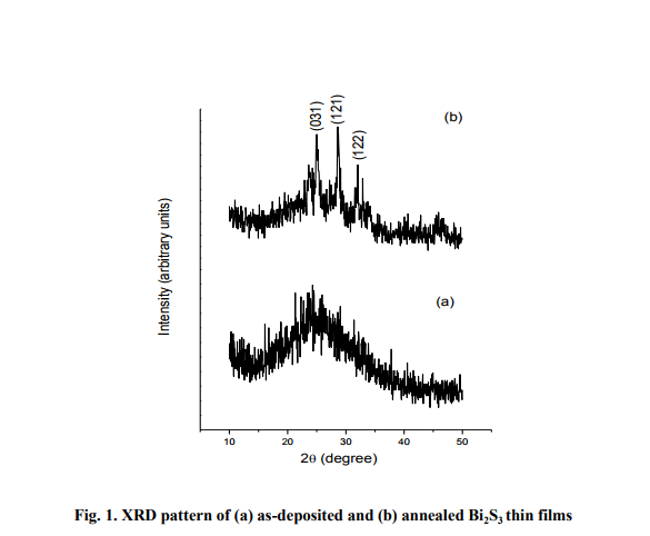
X-ray diffraction pattern of thermally evaporated Bi2S3 thin film is shown in fig. 1. No significant peaks are observed in the case of as-deposited films, thereby indicating amorphous nature of the films. On vacuum annealing at 200°C for an hour, amorphous Bi2S3 thin films transformed to polycrystalline, which is evidenced by the appearance of prominent peaks in the XRD pattern. Jolly Lukose et al 1991observed that the crystallisation of Bi2S3 thin films is partial at 150°C and complete at 200°C. The peaks are indexed by comparing the peak positions with the standard data. The XRD pattern of vacuum annealed Bi2S3 thin films matched well with the standard powder diffraction data of Bismuthinite (JCPDS-84 0279). The Bi2S3 thin films are found to exhibit orthorhombic crystal structure and the calculated value of lattice parameters are a=3.980 Å, b=11.158 Å, c=11.382 Å. Estimation of particle size (t) based on the X-ray diffraction peak broadening is done using Scherrer formula [Cullity 1956], t = 0.9 λ / (βhkl cos Θ hkl) (2) where, λ is the wavelength of X-rays used (1.5406 Å), βhkl is the angular width of the peak at half maximum intensity for the (hkl) plane and θ hkl is the Bragg angle corresponding to (hkl) plane.
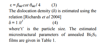
The average size of the particles in the annealed films of different thickness range from 20-30 nm. It is also observed that thicker films consisted of larger particles and vice versa. From the knowledge of ?t‘ and ?βhkl‘ the micro strain (ε) developed in the Bi2S3 thin films is calculated using the relation [Poulomi Roy et al 2006]

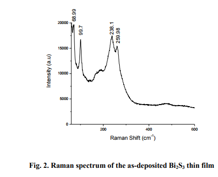
Laser Raman Spectroscopy is an effective method for the microstructural investigation of the materials. Raman spectrum of the typical asdeposited Bi2S3 film of thickness 103 nm is shown in fig. 2. The film exhibits characteristic Raman peaks at 69.88, 100.4, 238.3, 260.1 cm-1 and the peak positions agree well with the reported values in the literature [Chunjuan Tang et al 2010]. The peak at 260.1 cm-1 is attributed to the vibration of Bi-S bond [Chalermchai
Pilapong et al 2010]. The Raman spectrum of the film with characteristic peaks proves the definite phase formation in vacuum evaporated Bi2S3 thin films.
3.3 AFM Analysis
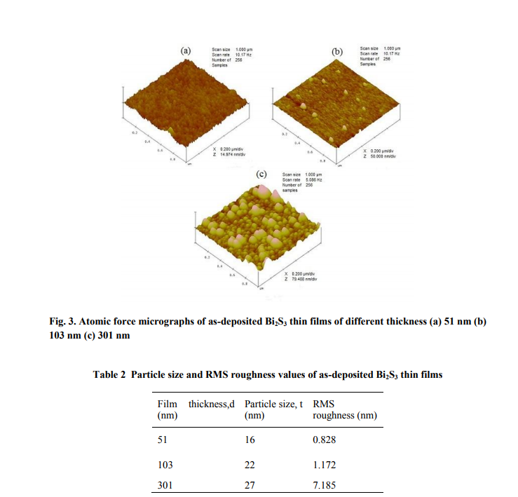
The atomic force micrographs of the asdeposited Bi2S3 thin films are shown in fig. 3. The as-deposited films consisted of nanosized particles and their aggregates. The software ?Nanoscope Control 6.13? is used to determine the size of particles from the atomic force micrographs. The estimation of RMS roughness is an added tool for the analysis of thin film surface, which is calculated, in the present study using the above said software. The observed RMS roughness and particle size of the asdeposited films are given in Table 2.
3.4. Optical properties
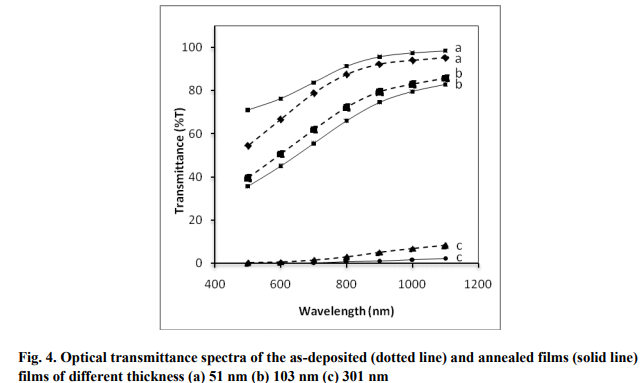
The optical transmittance spectra of the asdeposited and annealed samples are shown in fig. 4. The films are highly transparent at longer wavelengths. The transmittance of the films decreased with annealing but the film of thickness 51 nm became more transparent upon annealing. The optical constants such as absorption index and absorption coefficient are calculated from the transmittance data. The absorption coefficient (α) is determined from transmittance (T) values using the following relation [Subramanian et al 2010] α = (1/t)*ln(1/T) (5) where ?t‘ is the thickness of the film. The optical band gap energy of the films is calculated using the classical relationship [Tauc et al 1966] for near edge optical absorption in semiconductors αhν= K (hν-Eg) n/2 (6) (6) where K is a constant, hν is photon energy, Eg is the optical band gap and ?n‘ is a constant equal to 1 for direct band gap and 4 for indirect band gap compounds.
An extrapolation of the linear region of the plot of (αhν) 2 vs. hν gives the value of optical band gap, Eg when (αhν) 2 =0. The direct allowed transitions taking place in the film are confirmed by the linear nature of the (αhν) 2 vs. hv plot as shown in fig. 5. The band gap of the annealed films is lower than the band gap of the asdeposited films which may be attributed to the improvement of particle size after annealing. Similar results are obtained by Mane et al 1999 for the Bi2S3 thin films deposited by chemical method. Sonawane et al 2007 obtained a band gap of 1.717 eV for stoichiometric Bi2S3 thin film while the Eg value changed to 3.657 and 1.408 eV respectively for bismuth rich and sulphur rich films prepared by chemical bath deposition method.
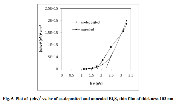
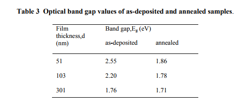
In the present study, the band gap values of the films of different thickness varied from 2.55- 1.76 eV and 1.86-1.71 eV respectively for asdeposited and annealed films. The calculated band gap values are listed in Table 3. Ublae 2010 obtained a band gap of 1.84-2.66 eV for the nanostructured Bi2S3 thin films, having thickness in the range of 201- 45 nm.
4. CONCLUSION
Polycrystalline Bi2S3 thin films are deposited by single source thermal evaporation technique and the microstructural and optical properties of films are analysed. Post deposition vacuum annealing of the films at 200°C improved the structural and optical properties of films. The microstructural parameters of the Bi2S3 thin films exhibiting orthorhombic crystal structure are evaluated and are found to be dependent on thickness. The Raman spectra of the film exhibited relevant peaks thereby indicating definite existence of Bi2S3 material. The optical transitions taking place in the material are found to be direct and allowed. The band gap value of as-deposited and annealed films of different thickness is in the range of 2.55-1.71 eV.
ACKNOWLEDGEMENT
The authors gratefully acknowledge Prof. Ajay Gupta, Centre director, UGC-DAE CSR, Indore Centre, for providing characterization (XRD, SEM, AFM, UV-Vis. and Raman) facilities and Department of Science and Technology, Govt. of India for the financial support.
References:
1. Atanu Jana, Chinmoy Bhattacharya, Subrata Sinha, Jayanti Datta, 2009, J. Solid State Electrochem., 13, 1339
2. Benramdane N., Latreche M., Tabet H., Boukhalfa M., Kebbab A., Bouzidi A., 1999, Mater. Sci. Eng., B 64, 84
3. Biljana Pejova, Ivan Grozdanov, 2006, Mater. Chem. Phys., 99, 39
4. Chalermchai Pilapong, Titipun Thongtem, Somchai Thongtem, 2010, J. Phys. Chem. Solids, 71, 712
5. Chunjuan Tang, Changqing Wang, Fengjian Su, Chunhe Zang, Yanxin Yang, Zhengjun Zong,Yongsheng Zhang, Solid State Sci. (2010),doi: 10.1016/j.solidstatesciences.2010.05.007
6. Cullity B.D., 1956, Elements of X-ray diffraction,USA , Addison-Wesly, 261
7. Jolly Lukose, Pradeep B., 1991, Solid State Commun., 78, 535 8. Mane R.S., Sankapal B.R., Lokhande C.D., 1999, Mater. Chem. Phys., 60, 196
9. Poulomi Roy, Suneel Kumar Srivastava, 2006, Thin Solid Films, 496, 293
10. Richards D.W., De Angelis R.J., Kramer M.P., House J.W., Cunard D.A., Shea D.P., 2004, Adv. X-ray Analysis, 47, 351
11. Rincon M.E., Sanchez M., George P.J., Sanchez A., Nair P.K., 1998, J. Solid State Chem.,136,167
12. Subramanian S.,Chitra lekha P., Pathinettam Padiyan D., 2010, J. NonCryst. Solids, 356,1173
13. Sonawane P.S., Patil L.A., 2007, Mater. Chem. Phys., 105, 157
14. Tauc J., Grigorovici R., Vancu A., 1966, Phys. Status Solidi, 15, 627
15. Ubale A.U., Daryapurkar A.S., Mankar R.B., Raut R.R., Sangawar V.S., Bhosale C.H., 2008, Mater. Chem. Phys., 110, 180 16. Ubale A.U., 2010, Mater. Chem. Phys. 121, 555
|


 This work is licensed under a Creative Commons Attribution-NonCommercial 4.0 International License